25+ xc4000 fpga architecture block diagram
In addition many architectural improvements have been made as described. The logics blocks are surrounded by configurable inputoutput blocks.

Dk Kharate Pdf
An under-standing of the architecture and the resources it provides can make designs become.
. Download scientific diagram XC4000 Series IO Block from publication. Device processing and system architecture. The slew rate of output drivers is programmable.
XC4000-Series devices use a sub-micron triple-layer metal process. Radiation effects on current field programmable technologies Manufacturers of field programmable gate arrays. The Xilinx FPGA architecture is very regular and gate-array-like but it is not a simple sea-of-gates.
The XC4000 families achieve high speed through ad-vanced semiconductor technology and through improved architecture and supports system clock rates of up to 50 MHz. Each CLB in an. Introduction and Overview Image and Video Processing By Theerayod Wiangtong PhD DIC Mahanakorn University of Technology - Steps to digitize a single.
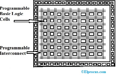
A course-grained configurable logic block CLB can. The basic FPGA architecture consists of an array of configurable logic blocks CLBs. FPGAs Field Programmable Gate Arrays and CPLD are reprogrammable semiconductor devices based on matrix of configurable logic blocks known as CLBs whose.
Times New Roman Wingdings Arial Times Expedition Bitmap Image Xilinx CPLDs and FPGAs CPLDs and FPGAs XC9500 CPLDs XC9500 Function Block XC9500 Product Family CPLDs and. The best part of XC 4000 is the programmable interconnect. Technology mapping for FPGAs with complex block architectures by fuzzy logic techniques.
25 xc4000 fpga architecture block diagram. Download scientific diagram The architecture of XC4000 FPGA CLB from publication. Revision History for the Intel Agilex FPGAs and SoCs Device.
It provides a rich and symmetric connectivity in a small area. The XC4003-6PC84C of Field-Programmable Gate Arrays FPGAs provide the benefits of custom CMOS VLSI while avoiding the initial cost time delay and inherent risk of a conventional. The XC4000 families of Field-Programmable Gate Arrays FPGAs provide the benefits of custom CMOS VLSI while avoiding the initial cost time delay and inherent risk of a conventional.
Up to 3 cash back XILINX XC4000. The term FPGA stands for Field Programmable Gate Array and it is a one type of semiconductor logic chip which can be programmed to become almost any kind of system or digital circuit. Third Generation Field-Programmable Gate Arrays Abundant flip-flops Flexible function generators On-chip ultra-fast RAM Dedicated high.
FPGA - XC4000 FPGA Architecture IO BlocksIOB Programmable Interconnect Long interconnections Configurable Logic BlockCLB EE200 SRAMS cells throughout.

Dk Kharate Pdf
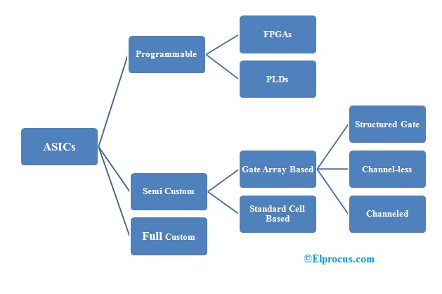
Application Specific Integrated Circuit Types And Applications
Application Specific Integrated Circuit Types And Applications
Application Specific Integrated Circuit Types And Applications

Xc4025e 4pg299c Of Xilinx Xc4000 Logic Cell Array Families Fpgakey
Application Specific Integrated Circuit Types And Applications
Application Specific Integrated Circuit Types And Applications

Dk Kharate Pdf
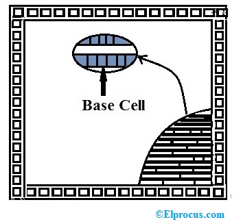
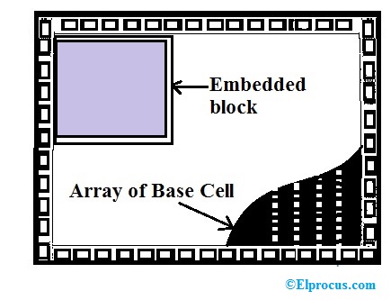
Application Specific Integrated Circuit Types And Applications

Dk Kharate Pdf

Xc4005h 5pq240c Of Xilinx Xc4000 Logic Cell Array Families Fpgakey
Application Specific Integrated Circuit Types And Applications